
Enabling The Development Of Powerful Yet Compact Devices

Enabling The Development Of Powerful Yet Compact Devices
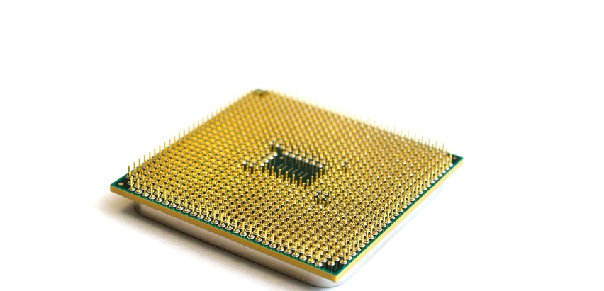
Core Components of VLSI Design

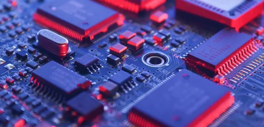
Major VLSI Design Domains:
- Digital VLSI Design – Focuses on logic gates, finite state machines, processors, and data paths.
- Analog VLSI Design – Includes op-amps, ADCs/DACs, and RF circuits.
- Mixed-Signal Design – Combines both analog and digital components on a single chip (common in sensors and audio processors).
- Hardware Description Languages (HDLs): Verilog and VHDL are used to model and simulate circuit behavior before physical design. RTL (Register Transfer Level) design allows defining how data moves and gets processed in the chip.
- Verification & Testing: Functional Verification – Ensures the design meets intended logic. Static Timing Analysis (STA) – Checks if the chip meets speed and timing constraints. DFT (Design for Testability) – Adds extra logic to test chips after manufacturing.
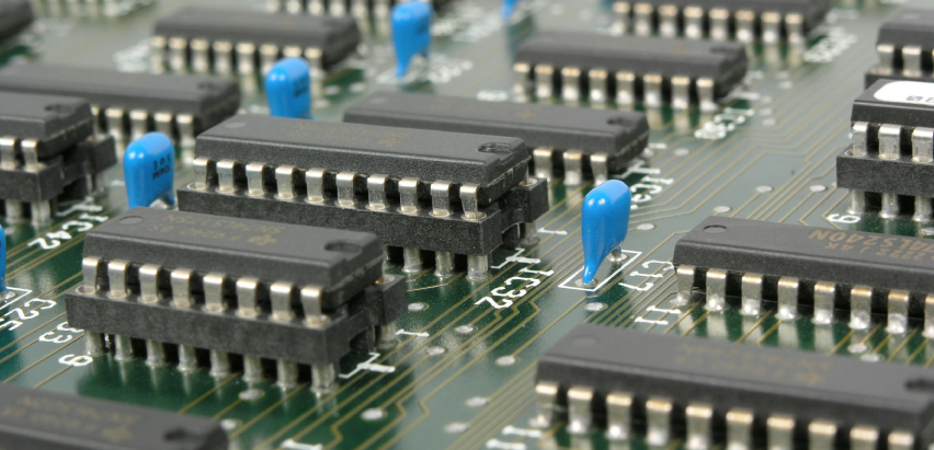
- VLSI Fabrication Process: After the design phase, the chip is sent for fabrication—a highly precise process involving: Photolithography Etching Doping Metallization Packaging
Trending Areas in VLSI:
AI & Machine Learning Accelerators
Recent post